
HDI PCB Development
The global HDI PCB market is characterized by ongoing technological advancements, the expansion into emerging applications and regions and connectivity trends such as 5G and IoT. Additionally, there is a push towards greater collaboration and standardization within the industry which has a direct impact on design, manufacturing and end-of-life strategies. In addition to these factors, manufacturers of high-density interconnect boards have to address the challenges of integrating circuitry and ensuring reliability in a small footprint.
Miniaturization Requirements: The trend towards compact electronic gadgets with increased functionality and performance is the primary driver of demand for high-density interconnect solutions. The fine lines and spaces, micro vias, and multiple layers enabled by HDI technology meet these requirements by packing in more elements into a smaller space.
Embedding Advanced Technologies: With the proliferation of 5G networks and IoT devices, the demand for hdi board has been increasing rapidly due to their ability to provide high-speed data transmission, low latency and reliability. HDI PCBs are also capable of handling RF signals making them suitable for incorporating RF components like antennas in smartphones.
Sustainability: There is a growing emphasis on environmental responsibility in all sectors, and the electronics industry is no exception. As such, there is a need for the industry to be more sustainable in its production processes. This can be achieved through the use of recyclable materials and adopting best practices in the design and manufacture of circuit boards. Additionally, manufacturers need to focus on the design of end-of-life electronic waste management programs which will help minimize the burden on local governments and the environment.
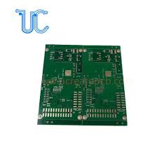
Future Trends in HDI PCB Development
Several innovations have been introduced in the production of HDI PCBs, including laser drilling and sequential build-up (SBU) processes. These advances have facilitated the creation of finer lines and spaces and microvias in HDI PCBs, leading to improved signal integrity and electrical performance. Additionally, these innovations have reduced the thickness of metallization on PCBs, allowing for higher density and more efficient power transmission.
A comprehensive quality control process is vital to ensuring the precision and reliability of HDI PCBs. This can be achieved by implementing rigorous testing protocols for aspects such as impedance control, solder joint integrity and the integrity of signal transmission. Furthermore, implementing robust design and engineering techniques can further improve the quality of the board. These include selecting appropriate materials with specific dielectric properties and careful consideration of component placement, trace routing and via structures. This will allow engineers to optimize the performance of HDI PCBs while maintaining a compact footprint.
HDI boards are typically made from advanced materials that have superior electrical properties compared to standard PCB materials. These materials help reduce signal loss and electromagnetic interference (EMI), ensuring the reliable operation of the circuits within. Common materials used in HDI boards include high-frequency laminates, PTFE (Teflon), and ceramic-based substrates, which provide excellent insulation, durability, and high-speed performance.
Consumer electronics such as laptops, gaming consoles, and wearables require high-performance circuitry in compact devices. HDI boards allow these electronics to meet the increasing performance demands of modern users, including faster processing speeds, improved battery life, and enhanced connectivity.