
PCB HDI
For complex printed circuit boards (PCBs), High-Density Interconnect (HDI) techniques are used to increase routing density without affecting signal quality. As a result, HDI designs require thinner traces and spaces. These smaller features are difficult to manufacture and require higher precision. They are also more susceptible to environmental factors, like thermal cycling and reflows, which can affect their performance over time. This is why it is important to consider the stackup design and materials when designing an HDI board.
The max layer count for PCB HDI depends on the component densities and pin counts required by the device. For example, a BGA component has more pins and requires more layers to route them all away from the package. This means the PCB must have at least a 16-layer stack-up in order to ensure adequate routing capacity.
The deciding factors for choosing an optimal pcb hdi stackup are the board’s performance requirements, manufacturability constraints and cost considerations. A high-quality material with a low dielectric loss is essential for achieving excellent signal performance. In addition, the copper foil thickness plays a key role in how well a PCB can withstand high temperatures and reflows.
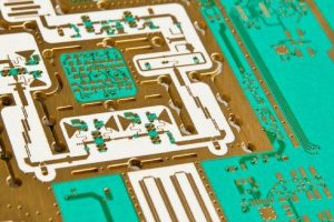
Max Layer Count For PCB HDI
A successful HDI design depends on a number of factors including the layer stack-up, via architecture, BGA fanout, and routing efficiency. It is also important to consider the fabrication process and its capabilities in terms of both etching and drilling of holes. In addition, it is necessary to choose a high-quality dielectric with the appropriate maximum withstanding temperature and CTE.
Another consideration when designing an HDI board is the stack-up sequence and its implications for signal integrity. It is recommended to use a sequential stack-up structure where possible. This allows for the use of microvias and reduces signal propagation delays due to reflows. Additionally, the layer stack-up sequence can impact the metallization of the final product. For example, a lower-layer dielectric can allow for faster and more accurate etching of the copper layer.
The aspect ratio of laser-drilled microvias is a critical factor in an HDI design. It is recommended to keep this ratio below 1:1 to ensure reliable fabrication. It is also important to stagger the placement of the vias in order to minimize stress points and avoid impedance problems.
Finally, a successful HDI design requires careful coordination of the power and ground planes. It is recommended to keep the power and ground planes as close to the signal layers as possible to ensure effective decoupling. In addition, it is a good idea to use alternate power and ground reference planes for optimal signal integrity.
A successful HDI design is a combination of many different aspects, all of which work together to achieve the desired functionality. By following the guidelines outlined in this article, designers can create a board that is both high-performance and easy to manufacture. This is a must for any electronic device that requires high-speed communication between its components. By taking the time to design an efficient HDI layout, engineers can avoid expensive manufacturing errors and keep their designs running as smoothly as possible.